Specification of Multi-crystalline Silicon Wafer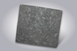
Conductivity Type: P-Type
Crystallinity :Multi-crystalline
Crystal size :≤50 crystals per 2 cm2
Oxygen (atoms/cm3): ≤8.0 x 10¹⁷
Carbon (atoms/cm3): ≤5.0x 10¹⁷
Resistivity (Ω·cm): 0.5~2.0
Dopant: Boron
Life time(μs) : ≥2.0
Dimensions Tolerance (mm) :156x156 ±0.5
Wafer dull (mm) :1.5±0.5
Center Thickness (μm) :200±20
Total Thickness Variation (μm): ≤20
Warp(μm): ≤40
Wafer cleaning :Water+detergent
Water slicing:Glycol based wafering
Saw marks(μm):Depth ≤15
Edge defect(through wafer) Length ≤5 mm,width ≤0.5 mm
packaging bubble:carton and wooden box
Payment:T/T,L/C
Supply Ability:10,000,000 pcs/month
Pcakage:1800 pcs/carton
300 pcs/box